Showing posts sorted by date for query high frequency. Sort by relevance Show all posts

Thursday, May 16, 2024

PCB Etching Compensation For Manufacturing

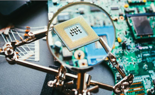
Introduction to Etching Compensation

One critical step in the PCB manufacturing process is etching, where unwanted copper is removed to form the desired circuit patterns. However, during etching, factors such as chemical reactions and process variations can cause deviations from the intended design. This is where etching compensation comes into play.

PCB Etching


Etching compensation involves adjusting the dimensions of the artwork to account for material removal during the etching process. By pre-emptively altering the trace widths and spacing on the design files, manufacturers can ensure the final product closely matches the intended specifications. This compensation is crucial for maintaining the electrical performance and reliability of the PCB.

The importance of etching compensation cannot be overstated. Precise control over the trace widths and spacing is essential for achieving the desired electrical characteristics, such as impedance and signal integrity. Without proper compensation, the etched traces could end up too narrow or too wide, leading to potential failures in the electronic device.

In this blog, we will explore why etching compensation is necessary, its impact on impedance, the relevant IPC standards, how manufacturers handle compensation for high-speed PCB and high-frequency PCB, and best practices to achieve optimal results.

Why Etching Compensation is Necessary from a PCB Manufacturing Perspective

The etching process involves several steps, including coating the PCB with a photoresist, exposing it to a pattern, developing the exposed resist, and finally etching away the unprotected copper. Despite advancements in manufacturing technology, the etching process is still subject to various factors that can affect the precision of the trace widths and spacing. These factors include:

  • Chemical concentration: Variations in the concentration of the etching solution can lead to uneven material removal.
  • Temperature fluctuations: Changes in temperature can affect the rate of chemical reactions, causing inconsistencies in etching.
  • Process duration: The time the PCB is exposed to the etching solution can impact the amount of copper removed.
  • Equipment calibration: Inaccuracies in the calibration of etching equipment can lead to deviations from the desired dimensions.

These challenges make it difficult to achieve the precise trace widths required for modern PCBs. Without etching compensation, the final traces may be too thin, leading to increased resistance, reduced current-carrying capacity, and potential overheating. Conversely, traces that are too wide can result in crosstalk, signal interference, and compromised circuit performance.

Etching compensation addresses these issues by adjusting the original artwork to account for the expected material removal. By doing so, manufacturers can produce PCBs that meet the stringent requirements of electronic devices, ensuring reliable operation and long-term durability.

Will Etching Compensation Affect Impedance Output?

Impedance is a critical parameter in PCB design, especially for high-frequency and high-speed applications. It refers to the resistance to the flow of alternating current (AC) in a circuit and is influenced by the trace width, trace thickness, and the dielectric properties of the PCB material. Maintaining the correct impedance control is essential for signal integrity and minimizing signal loss.

Etching compensation directly impacts impedance because it alters the trace widths. If the compensation is not done correctly, the resulting traces may not match the intended impedance, leading to signal integrity issues. For instance, if the traces are narrower than designed, the impedance will be higher, causing signal reflections and potential data errors. Conversely, wider traces result in lower impedance, which can also degrade signal quality.

Manufacturers address this by carefully calculating the amount of compensation needed to achieve the desired impedance. This involves:

  • Pre-compensation calculations: Determining the expected material removal and adjusting the trace widths accordingly.
  • Test coupons: Creating test structures on the PCB that can be measured to verify the actual impedance after etching.
  • Iterative adjustments: Fine-tuning the compensation parameters based on the test results to ensure the final traces meet the impedance requirements.

By implementing these strategies, PCB manufacturers can ensure that etching compensation does not adversely affect impedance, maintaining the signal integrity and performance of the PCB.

IPC Etching Tolerance from Original Artwork

The IPC sets the standards for PCB design and manufacturing to ensure consistency, reliability, and quality across the industry. One such standard is IPC-6012, which specifies the performance and qualification requirements for rigid PCBs. Within this standard, there are guidelines for etching tolerance, which refer to the allowable deviations from the original artwork dimensions.

According to IPC-6012, the etching tolerance typically ranges from ±10% to ±20% of the trace width. This means that if a trace is designed to be 10 mils wide, the actual width after etching should be within 9 to 11 mils for a ±10% tolerance. Adhering to these standards is crucial for ensuring that the PCB meets the design specifications and performs as intended.

Manufacturers use these standards as a benchmark for their etching processes. By following the IPC guidelines, they can produce PCBs that are consistent in quality and performance, reducing the risk of failures and ensuring customer satisfaction.

How Factories Control Their Etching Compensation for High-Speed or High-Frequency PCBs

High-speed and high-frequency PCBs present unique challenges for etching compensation. These PCBs require tighter control over trace widths and spacing to maintain signal integrity and minimize losses. Factories employ several techniques to achieve the necessary precision:

  • Advanced photolithography: Using high-resolution photomasks and precise exposure equipment to create accurate patterns on the PCB.
  • Automated process control: Implementing automated systems to monitor and adjust the etching process in real-time, ensuring consistent results.
  • Regular calibration: Frequently calibrating equipment to maintain accuracy and prevent deviations from the desired dimensions.
  • Statistical process control (SPC): Using statistical methods to analyze process data and identify trends or anomalies, allowing for proactive adjustments.

By leveraging these techniques, manufacturers can effectively control etching compensation for high-speed and high-frequency PCBs, ensuring that the final products meet the stringent performance requirements of modern electronic devices.

Best Practices for Etching Compensation

Achieving optimal results in etching compensation requires collaboration between PCB designers and manufacturers. Here are some best practices to consider:

  • Design for manufacturability (DFM): Incorporate etching compensation into the design phase, considering the manufacturing capabilities and limitations.
  • Use of simulation tools: Utilize software tools to simulate the etching process and predict the necessary compensation adjustments.
  • Regular communication: Maintain open lines of communication between designers and manufacturers to address any issues or changes in the design or process.
  • Continuous improvement: Implement a feedback loop to review the performance of the etching process and make continuous improvements.

By following these best practices, both designers and manufacturers can ensure that etching compensation is effectively implemented, resulting in high-quality PCBs that meet the demands of modern electronic devices.

Friday, May 10, 2024

Copper in PCBs: Clad Laminate to Plating Techniques

Copper is fundamental in the realm of printed circuit boards (PCBs), Its exceptional electrical conductivity, flexibility, and thermal properties make it indispensable across various applications, from simple electronic devices to complex systems in the automotive and renewable energy sectors. This blog delves deep into the nuances of copper clad laminates and copper foil rolls, providing insights into copper plating techniques, IPC standards for copper thickness, and the balance of cost versus performance in high-power applications. Each section is tailored to equip electronics engineers and PCB designers with the latest advancements and comparative analyses necessary for optimizing PCB design and functionality.

Copper Clad and plating


Copper Clad Laminate and Foil Roll


What are Copper Clad Laminates?

Copper clad laminates (CCL) are critical materials used in the fabrication of printed circuit boards. Consisting of an insulating base material and copper foil, they form the foundational layers onto which circuitry is etched. The selection of a suitable CCL can profoundly impact the performance, durability, and cost-efficiency of the final PCB product.

The base material in a CCL is typically made from fiberglass, epoxy resins, or other composite materials, which provide the mechanical strength and insulation required for stable circuit operation. The copper foil, adhered to this base, is where the actual circuit paths are created during the PCB manufacturing process. The thickness and purity of this copper layer are pivotal in determining the board’s conductivity and ability to withstand thermal stress.

Types of Copper Foil Rolls

Copper foil rolls are available in various grades and thicknesses, each suited to specific applications:

  • Electrodeposited (ED) Copper Foil: Produced through an electrochemical process, ED copper foil offers excellent ductility and uniform thickness, making it ideal for fine-line printing and multilayer PCBs.
  • Rolled Annealed (RA) Copper Foil: Made by mechanically rolling copper to the desired thickness, RA foil is less ductile than ED but provides superior flexibility and fatigue resistance, beneficial for flexible PCBs.

Applications in PCB Manufacturing

The choice between different types of copper foil affects the PCB's performance in several ways:

  • Signal Integrity: Thinner foils are generally used where high-frequency performance is critical, as they provide reduced impedance.
  • Thermal Management: Thicker copper foils can handle higher current loads, making them suitable for power electronics and automotive applications where heat dissipation is crucial.
  • Cost-Efficiency: The cost of copper foil impacts the overall manufacturing budget, with choices often reflecting a balance between performance requirements and material expenditures.

The integration of quality copper clad laminates with appropriate copper foil types is fundamental to achieving reliable and efficient PCBs. As we explore further, understanding these materials' properties and the innovative techniques applied in their use will reveal how they contribute significantly to advancements in PCB technology.

Copper Foil Types in PCB Fabrication

The performance of a PCB largely hinges on the type of copper foil used. Each type offers unique benefits and limitations, influencing its suitability for various applications. A comparative analysis of the most common types—Electrodeposited (ED) and Rolled Annealed (RA)—sheds light on these distinctions.

Electrodeposited (ED) Copper Foil

Electrodeposited copper foil is manufactured through an electrochemical process that ensures a uniform thickness across its surface. This uniformity is crucial for high-frequency PCB applications where consistency in electrical properties is paramount.

Advantages:

  • Uniform Thickness: Promotes consistent electrical characteristics across the PCB.
  • Fine Line Capability: Suitable for intricate circuit designs due to its precision in thickness and line formation.
  • Cost-Effectiveness: Generally less expensive than RA copper due to its simpler manufacturing process.

Disadvantages:

  • Lower Mechanical Strength: More prone to tearing during handling and processing, which can be a drawback in mechanically demanding applications.

Rolled Annealed (RA) Copper Foil

Rolled Annealed copper foil is created by mechanically rolling the copper to achieve the desired thickness, followed by an annealing process to enhance its flexibility. This method imparts a higher mechanical strength to the foil, making it ideal for applications requiring repeated flexing.

Advantages:

  • High Flexibility and Strength: Better suited for flexible PCBs used in dynamic applications.
  • Thermal Stability: Offers superior resistance to thermal degradation during soldering and other high-temperature processes.

Disadvantages:

  • Higher Cost: The additional processing steps make RA copper more expensive.
  • Thickness Variability: Can exhibit slight variations in thickness, which might affect impedance in sensitive circuits.

Choosing the Right Copper Foil

The choice between ED and RA copper foils depends on several factors:

  • Circuit Complexity: ED is preferred for complex, fine-line circuits.
  • Application Flexibility: RA is chosen for circuits requiring mechanical flexibility.
  • Budget Constraints: ED is more budget-friendly, though RA may offer longer lifecycle savings in demanding environments.

IPC Standard for Copper Plating

Adherence to industry standards is critical in PCB manufacturing to ensure quality and reliability. The IPC 6012 standard provides guidelines for copper plating thickness for both inner and outer layers of PCBs, which are pivotal in determining the board's performance and longevity.

Inner Layer Copper Thickness


Standard Thickness: Typically ranges from 0.5 oz/ft² to 2 oz/ft². The thickness is chosen based on the current-carrying capacity and thermal management needs of the application.

IPC Guidelines: Refer above IPC table. Ensure sufficient copper thickness to handle the expected electrical load without excessive voltage drop or overheating.

Outer Layer Copper Thickness

Copper plating Outer


  • Standard Practices: Outer layers generally require thicker copper, ranging from 1 oz/ft² to 3 oz/ft², to accommodate surface mount technology (SMT) and through-hole component mounting.
  • IPC Considerations: Refer above IPC table. Emphasizes durability and connectivity, especially for external connections that may be subject to mechanical stress.

Implications for PCB Design

  • Signal Integrity: Adequate copper thickness is essential for maintaining signal integrity, particularly in high-speed applications.
  • Thermal Management: Thicker copper layers efficiently dissipate heat, crucial in high-power applications and in reducing hotspots on the PCB.

These sections provide a detailed exploration of copper foil types and standards critical for optimizing PCB design and manufacturing. Let me know if this meets your expectations, or if there are additional points you'd like to include before I continue with the next sections on advancements in copper plating techniques and their applications.

Advancements in Copper Plating Techniques for Enhanced PCB Performance

Copper plating technology has seen significant advancements aimed at improving the reliability and efficiency of printed circuit boards. These developments are not only crucial for enhancing the electrical characteristics of PCBs but also play a pivotal role in environmental sustainability and manufacturing precision.

Improved Plating Methods

Direct Current (DC) Plating: Traditionally used for its simplicity and cost-effectiveness, DC plating involves applying a direct current to deposit copper onto the substrate. Recent improvements have focused on enhancing the uniformity and adhesion of the copper layer.

Pulse Reverse Plating: An advanced technique that alternates between forward and reverse current pulses. This method improves the distribution of copper, particularly in high-density interconnect (HDI) PCBs, by allowing better control over the deposition process, leading to finer grain structures and reduced void formation.

Benefits of Advanced Copper Plating

Increased Durability: Enhanced plating techniques contribute to a stronger bond between the copper and the substrate, which is critical in environments subjected to thermal and mechanical stress.

Higher Conductivity: Uniform copper deposition improves overall board conductivity, crucial for maintaining signal integrity in high-frequency applications.

Environmental Impact: Advances in plating technology often focus on reducing chemical waste and improving energy efficiency, aligning with the growing demand for green manufacturing processes.

The Role of Copper in PCB Signal Integrity and The Impact of Copper Thickness on PCB Heat Management

Copper's role in PCB manufacturing extends beyond its electrical conductivity; it is also fundamental in maintaining signal integrity and managing heat within circuit operations.

Copper and Signal Integrity

  • Minimizing Signal Loss: Copper's excellent conductive properties help in minimizing signal loss across the circuit, which is essential for maintaining the performance of high-speed PCBs.
  • Reducing Crosstalk: Properly managed copper thickness and placement can significantly reduce electromagnetic interference (EMI) and crosstalk between circuit elements, improving overall circuit reliability.

Copper Thickness and Heat Management

Enhanced Heat Dissipation: Thicker copper layers facilitate better heat dissipation, crucial for preventing hot spots and thermal damage, especially in dense, high-power circuits.

Design Considerations: Designers must balance copper thickness with board flexibility and weight, as excessive copper can lead to issues with board handling and increased material costs.

Balancing Cost and Performance in High-Power Applications: Automotive and Renewable Energy Sectors

In sectors like automotive and renewable energy, where reliability and efficiency are paramount, the use of copper in PCBs must be strategically balanced against cost considerations.

Automotive Industry Applications

  • Reliability Under Harsh Conditions: Copper's thermal and electrical stability makes it ideal for automotive electronics, which often operate under extreme environmental conditions.
  • Innovations in Safety and Performance: Advanced copper usage in vehicle electronics improves safety features and performance metrics, directly influencing consumer satisfaction and adherence to safety regulations.

Renewable Energy Industry Applications

  • Maximizing Efficiency: In renewable energy applications, such as solar panels and wind turbines, copper plays a crucial role in minimizing energy loss and maximizing efficiency.
  • Longevity and Durability: The durability of copper ensures that devices can withstand environmental challenges over long periods, crucial for sustainable energy solutions.

Conclusion

The critical role of copper in the fabrication of printed circuit boards cannot be overstated. From copper clad laminates to advanced copper plating techniques, each component and process plays a pivotal role in enhancing the performance, durability, and efficiency of PCBs. As we have explored, the choice of copper foil—whether Electrodeposited or Rolled Annealed—and the adherence to IPC standards significantly influence the board's functionality and reliability in various applications.

Advancements in copper plating technologies not only promise improved electrical and mechanical performance but also point towards a more sustainable manufacturing process. These innovations are essential in meeting the growing demands for more complex and higher-performing electronic devices, especially in critical sectors like automotive and renewable energy. Here, copper’s ability to manage heat and maintain signal integrity ensures that systems operate at optimal levels, withstanding environmental stresses and minimizing energy loss.

As we look to the future, the ongoing development of copper application techniques in PCB manufacturing will undoubtedly continue to play a crucial role in the electronics industry. Engineers and designers are encouraged to stay abreast of these advancements, integrating cutting-edge copper technologies to stay competitive and fulfill the increasing demands for efficient, reliable, and robust electronic components.

In conclusion, the dynamic nature of copper usage in PCBs exemplifies the innovative spirit of the electronics manufacturing industry. By continuously refining copper's applications, the industry not only enhances the technical capabilities of electronic devices but also contributes significantly to their environmental sustainability. Thus, the journey of copper in PCB technology is far from complete, promising exciting developments and opportunities for years to come.

Thursday, May 9, 2024

Circuit Board Solder Mask

The solder mask serving as a thin protective layer that covers the majority of the circuit board's surface, the solder mask—also known as solder resist—plays a crucial role in ensuring both the functionality and longevity of the board. Its primary function is to prevent unintended solder bridges from forming between closely spaced solder pads, which can lead to short circuits and malfunctioning of the electronic components.

PCB Solder Mask


Beyond its protective attributes, the solder mask significantly influences the assembly process and the overall performance of the final product. Advances in this technology, including the development of inkjet and laser direct imaging techniques, have enhanced its precision and efficiency, aligning with the industry's move towards more compact and complex PCB designs. The ongoing evolution in solder mask technology not only supports higher density and higher frequency PCB applications but also drives the industry towards adopting more environmentally sustainable practices.

This post delves into the sophisticated world of solder masks, exploring their critical importance, technological advancements, and the standards governing their use. We will examine how these advancements contribute to enhanced PCB performance and reliability, particularly in high-density and high-frequency applications, and how the industry is shifting towards more sustainable practices.

Purpose and Importance of Solder Mask

Function of Solder Mask

The solder mask serves multiple critical functions in the lifecycle of a printed circuit board (PCB). Primarily, it acts as a protective barrier that guards the copper traces of the PCB from environmental factors such as dust, moisture, and oxidation, which can lead to corrosion over time. More importantly, the solder mask prevents the formation of solder bridges during the soldering process. Solder bridges occur when excess solder forms unintended connections between circuit elements, potentially causing short circuits and failures in electronic devices.

Moreover, the solder mask aids in the reduction of soldering errors by clearly defining where solder should be applied, improving manufacturing efficiency and reducing waste. It also provides a color contrast against the metal leads and pads, which is particularly useful during the inspection and testing phases of manufacturing, allowing for easy identification of flaws.

Testing Standards

Adherence to industry standards is paramount in PCB manufacturing, with specific requirements set forth for solder masks. The IPC SM 840 classifies solder masks based on their intended use and durability. This classification ensures that solder masks meet rigorous standards of thermal, chemical, and mechanical durability that align with the operational requirements of the final product.

For example, Class T solder masks are designed for general commercial use where the environment may not be harsh, whereas Class H is suitable for high-performance electronic products that are exposed to extreme environmental conditions. These standards are crucial for manufacturers to adhere to, ensuring reliability across various applications.

  • Thermal Endurance: Solder masks must withstand high temperatures during both the soldering process and the operational phase of the PCB.
  • Chemical Resistance: Effective resistance to the chemicals used in PCB manufacturing and operation, including cleaning agents and flux, is critical.
  • Mechanical Durability: The solder mask must be robust enough to resist scratching and other physical damages during handling and use.

The implementation of these standards is crucial not only for the functionality and longevity of the PCBs but also for maintaining high yield rates in PCB manufacturing, ultimately affecting the cost-efficiency of production and the reliability of the final products.

Next, I will cover the industry standards for solder mask thickness, explaining the typical ranges and their applications across various types of PCBs. This will include details on how thickness standards are determined and why they are important for different manufacturing requirements.

Standard Industry Thickness and Spec

Thickness Guidelines

The thickness of a solder mask can vary significantly depending on the application requirements of the printed circuit board (PCB). Generally, the standard thickness of solder masks ranges from 20 to 40 microns. However, specific applications may require adjustments to this range to accommodate different design and performance criteria.

The thickness is crucial because it impacts several aspects of PCB performance:

  • Insulation: Thicker solder masks provide better insulation, protecting against electrical shorts between closely spaced components.
  • Surface Planarity: A uniform solder mask thickness helps maintain a level surface for the mounting of components, which is particularly important in high-density interconnect (HDI) boards.
  • Durability: In environments where mechanical wear and abrasion are concerns, a thicker solder mask can offer enhanced protection, prolonging the life of the PCB.

Application-Specific Considerations

For standard applications, a thickness at the lower end of the range is often sufficient. However, for boards that are subject to harsher mechanical stresses or that require higher levels of insulation, the upper end of the thickness spectrum may be more appropriate.

  • High-Density Applications: In HDI PCBs, where the spacing between components is minimal, maintaining a thinner solder mask can prevent issues related to bridging and short-circuiting.
  • High-Frequency Applications: For high-frequency PCBs, the thickness of the solder mask must be carefully managed to avoid any adverse effects on the electrical properties of the board, such as impedance and capacitance.

Measurement and Compliance

The measurement of solder mask thickness is typically conducted using specialized equipment that can accurately gauge the coating on top of the copper traces and pads. It is essential for manufacturers to regularly verify this thickness to ensure compliance with both the design specifications and the relevant IPC standards.

Ensuring that the solder mask meets the specified thickness is vital not only for the functionality and reliability of the PCB but also for achieving optimal yield rates during manufacturing. By adhering to these standards, manufacturers can reduce the risk of defects, minimize rework, and maintain consistency across production batches.

Having detailed the industry standards for solder mask thickness and their importance in PCB manufacturing, I will next discuss how advancements in solder mask technology contribute to enhanced PCB performance and reliability, especially in high-density and high-frequency applications. This section will also explore the environmental impacts of different solder mask types and industry shifts towards more sustainable practices.

Technological Advancements in Solder Mask


Enhancements for High-Density Applications

Advancements in solder mask technology have significantly impacted the performance and reliability of PCBs, especially in high-density and high-frequency applications. Innovations such as Liquid Photo-Imaginable (LPI) solder masks and methods like Laser Direct Imaging (LDI) have allowed for greater precision in application, enabling finer resolution and better alignment with increasingly compact component layouts. These technologies ensure that the solder mask can effectively cover tiny pads while leaving the appropriate gaps for soldering, crucial for avoiding defects in densely packed circuits.

  • High-Frequency PCBs: For high-frequency applications, the properties of the solder mask, such as its dielectric constant and thickness, become even more critical. Advanced solder masks are designed to have minimal impact on signal integrity, reducing the risk of interference and signal loss which is paramount in high-frequency circuits.

Environmental and Sustainability Considerations

As the electronics industry moves towards more sustainable practices, the type of solder mask used plays a significant role. Traditional solder masks often involve the use of solvents and other chemicals that can be harmful to the environment. In response, manufacturers are shifting towards water-soluble or solvent-free formulations that reduce volatile organic compound (VOC) emissions.

  • UV Curable Solder Masks: These types of solder masks not only improve production efficiency by reducing curing times but also decrease energy consumption and environmental impact. UV curable masks require less energy and produce fewer emissions compared to traditional thermal curing processes.

Selecting Solder Mask Types

Selecting the right type of solder mask for a specific application involves considering various factors:

  • High CTI Solder Mask: Materials with a high Comparative Tracking Index (CTI) are better suited for environments where high voltage and humidity can cause electrical tracking and failure.
  • Halogen-Free Solder Masks: For applications requiring environmental and health safety, halogen-free solder masks are preferable as they do not release harmful halogens under high heat conditions.
  • Flexibility and Durability: Different applications may require solder masks with specific mechanical properties, such as flexibility for flex circuits or extra durability for industrial applications.
By considering these factors, designers and manufacturers can choose solder masks that not only meet the technical requirements of their PCBs but also align with environmental sustainability goals.

Next, I will detail what constitutes an Eco-Friendly Solder Mask, discussing its definition, benefits, and why its adoption is increasingly important in the context of global sustainability efforts within the electronics manufacturing industry.

Eco-Friendly Solder Mask Technologies


Definition and Benefits


An eco-friendly solder mask refers to a solder resist that minimizes environmental impact through its formulation and the manufacturing process it requires. These solder masks are typically made from materials that are less harmful to the environment, either by being free of volatile organic compounds (VOCs), halogens, and other hazardous substances, or by being biodegradable or recyclable. The primary benefits of using eco-friendly solder masks include:

  • Reduced Environmental Toxins: By avoiding harmful chemicals like brominated flame retardants or PVC-based compounds, eco-friendly solder masks reduce the release of toxins into the environment during both the manufacturing and disposal phases of the PCB lifecycle.
  • Lower Energy Consumption: Many eco-friendly solder masks are designed to cure at lower temperatures or through energy-efficient processes such as UV curing, which significantly reduces the energy consumption associated with their application and curing.
  • Compliance with Environmental Regulations: Using eco-friendly solder masks helps manufacturers comply with increasingly stringent environmental regulations and meet the certification standards required in many markets, enhancing product marketability.

Growing Industry Adoption


The adoption of eco-friendly solder masks is gaining momentum as the electronics industry seeks to enhance its sustainability practices. This shift is driven not only by regulatory pressures but also by consumer demand for more environmentally responsible products. As a result, more manufacturers are exploring green alternatives that align with their corporate social responsibility (CSR) goals.

  • Innovative Materials: Recent innovations include the development of solder masks derived from bio-based resins or those that utilize water-based technologies, further reducing their environmental footprint.
  • Market Differentiation: For PCB manufacturers, offering products made with eco-friendly solder masks can provide a competitive edge in markets where environmental sustainability is a significant concern among end-users.

The move towards eco-friendly solder masks reflects a broader trend in electronics manufacturing towards reducing ecological impacts and promoting sustainability without compromising the technical performance or reliability of the products.

Continuing from this discussion on eco-friendly solder mask technologies, the next section will delve into the various solder mask printing processes available in PCB manufacturing, such as stencil printing, spray methods, and others, highlighting their operational principles and suitability for different manufacturing scenarios.

Solder Mask Printing Processes


Overview of Methods


The application of solder masks to PCBs can be achieved through various methods, each with its unique advantages and best-fit scenarios. Understanding these methods is crucial for PCB manufacturers to select the most appropriate technology based on their specific production requirements and the complexity of the PCB designs they handle.

  • Stencil Printing Method: This process involves applying the solder mask using a stencil made to match the PCB layout. The mask is spread over the stencil, and excess is removed, leaving the mask only in the desired areas. This method is particularly effective for large-scale productions where consistency and speed are critical.
  • Spray Application Method: Spray methods utilize specialized equipment to spray the solder mask onto the PCB. This method provides a uniform and thin layer, which is ideal for high-density PCBs where precision is paramount. It is also adaptable to complex board shapes and sizes.
  • Curtain Coating: Another method is curtain coating, where the solder mask is poured over the PCB as it passes under a curtain of the mask material. This technique is efficient for achieving a consistent thickness across the board.
  • Dip Coating: In dip coating, the PCB is dipped into a tank containing the solder mask material, then withdrawn at a controlled rate to ensure a uniform coating. This method is suitable for boards requiring a thicker layer of solder mask.
  • Screen Printing: This traditional method involves pressing ink through a fine mesh or screen that is patterned according to the PCB design. Screen printing is versatile and cost-effective but less precise than newer technologies, making it less ideal for very fine or complex patterns.

Innovations


Recent advancements in solder mask application technologies include the development of more precise and efficient methods such as:

  • Laser Direct Imaging (LDI): LDI techniques allow for precise application of the solder mask without physical contact, using lasers to define the areas where the mask is needed. This method is excellent for complex, high-density PCBs where accuracy is critical.
  • Inkjet Printing: Inkjet technology in solder mask application offers high precision and the ability to apply the mask selectively, reducing waste and processing time. This method is particularly useful for prototypes and small-batch productions where flexibility and customization are required.
Each of these methods has its strengths and weaknesses, and the choice of which to use depends on factors such as the complexity of the PCB design, production volume, and cost considerations.

Next, I will discuss how the thickness of the solder mask affects the Impedance PCB and overall PCB stack-up thickness and provide insights into resolving issues related to impedance variations caused by different solder mask applications. This section will explore the technical challenges and solutions associated with integrating solder mask thickness into PCB design effectively.

Impact of Solder Mask Thickness on PCB Design


Impedance and Stack Up


The thickness of the solder mask can significantly influence the electrical properties of a printed circuit board (PCB), particularly its impedance. Impedance is a critical factor in high-frequency PCB designs, where precise control over signal integrity is essential. Variations in the thickness of the solder mask can alter the impedance values, potentially leading to signal integrity issues, such as reflections and crosstalk, which can degrade the performance of the board.

  • How Thickness Affects Impedance: The dielectric properties of the solder mask material and its thickness directly influence the impedance of the PCB. A thicker solder mask increases the distance between the signal layer and the reference plane, altering the impedance. This effect is particularly noticeable in controlled impedance applications, where maintaining consistent impedance values is crucial for the functionality of high-speed circuits.
  • Stack-Up Considerations: In multi-layer PCBs, the overall stack-up — the arrangement and thickness of the various layers — must be carefully designed to achieve the desired electrical characteristics and mechanical stability. The solder mask is an integral part of this stack-up, and its thickness needs to be considered in the overall design to ensure that the board meets the required specifications.

Solutions and Adjustments


To address the challenges posed by solder mask thickness variations, several strategies can be employed:

  • Impedance Modeling and Simulation: Advanced modeling and simulation tools can predict how changes in solder mask thickness affect impedance. By simulating different scenarios, designers can optimize the solder mask application to meet specific impedance requirements before the manufacturing process begins.
  • Material Selection: Choosing a solder mask material with appropriate dielectric properties is essential. Materials with lower dielectric constants may be preferable in designs where the solder mask thickness might impact impedance.
  • Process Control: Maintaining strict control over the application process of the solder mask can help minimize variations in thickness. This includes choosing the right application method and regularly calibrating equipment to ensure consistent results.
  • Design Adjustments: In some cases, adjustments to the PCB design may be necessary to compensate for the impedance effects of the solder mask. This could involve changing the layout of the signal paths or modifying the spacing between layers.

By understanding the implications of solder mask thickness and employing these solutions, PCB designers and manufacturers can effectively manage impedance variations and ensure the reliability and performance of their boards in high-frequency applications.

Conclusion


Solder mask technology is a cornerstone in the PCB manufacturing process, pivotal for both protecting the circuitry and enhancing the performance of the final product. As we have explored, the advancements in solder mask materials and application methods not only contribute to greater efficiency and precision in PCB production but also play a crucial role in meeting the high demands of modern electronic devices, especially those requiring high density and high frequency.

Furthermore, the shift towards eco-friendly solder masks reflects a broader movement within the electronics manufacturing industry towards sustainability. By adopting materials and processes that minimize environmental impact, the industry not only adheres to stricter environmental regulations but also meets the growing consumer demand for greener products.

For electronics engineers and PCB designers, staying informed about these trends and innovations in solder mask technology is essential. Whether it’s choosing the right type of solder mask to meet specific design requirements, understanding the implications of solder mask thickness on impedance, or selecting environmentally sustainable options, the choices made at the design stage can significantly affect both the performance and environmental footprint of the final product.

As we continue to push the boundaries of what's possible in electronics manufacturing, the evolution of solder mask technology will undoubtedly remain at the forefront, driving the development of more reliable, efficient, and sustainable electronic products.

Wednesday, May 1, 2024

Impedance Control In PCB Basic Guide

Impedance Control In PCB
Impedance control is a critical parameter in the design of printed circuit boards (PCBs), especially for applications involving advanced circuit boards such as high-speed signals and high-frequency environments. Proper impedance control ensures signal integrity and minimizes issues like signal reflection and cross-talk, which are vital for the reliability and performance of electronic systems. This post aims to demystify various aspects of impedance control, from basic concepts to advanced techniques, providing valuable insights for both novice and experienced PCB designers.

Understanding Impedance in PCBs

Trace Impedance refers to the resistance of a PCB signal trace at high frequencies. It is influenced by the trace width, thickness, the dielectric material around it, and the overall layout of the traces. Proper management of trace impedance is essential for maintaining signal integrity across the PCB.

  • Differential Pair Impedance involves two closely spaced traces carrying equal and opposite signals. The key to differential signaling is maintaining consistent impedance to ensure that the signals remain balanced, which is crucial for minimizing electromagnetic interference (EMI) and signal degradation.
  • Single End Impedance Control deals with the impedance of a single trace measured against a reference plane. It's crucial for the design of simpler, less costly PCBs where differential pairs are not feasible.

Material Impact on Impedance Control

The choice of PCB material significantly affects the accuracy of impedance control. Materials like FR-4 are commonly used due to their well-understood characteristics and cost-effectiveness. High-speed and high-frequency applications might require advanced pcb materials such as Rogers or Teflon that provide lower dielectric constants and loss factors, facilitating better impedance control.

PCB Layout for Better Impedance Control

Effective PCB layout is vital for achieving desired impedance levels. Key strategies include:

  • Trace Geometry: Adjusting the width and spacing of traces to match the target impedance.
  • Via Design: Optimizing via structures to minimize impedance discontinuities.
  • Routing Techniques: Using uniform trace routing to avoid impedance variations.

Optimal PCB Stackup Design

Designing an effective stackup is fundamental for multilayer PCBs, where each layer's configuration can impact overall impedance. A well-designed stackup helps in balancing the capacitive and inductive characteristics across the PCB, ensuring consistent impedance.

Impedance Control Techniques

Achieving precise impedance control involves several techniques, especially in multi-layer PCBs:

  • Simulation Tools: Utilizing PCB design software for impedance modeling and simulations.
  • Controlled Dielectric Materials: Selecting materials with consistent dielectric properties.
  • Impedance Testing: Implementing testing protocols to ensure the impedance matches the design specifications.

Challenges in Flexible Circuit Boards

Flexible PCBs pose unique challenges for impedance control due to their varying material properties and dynamic flexing. Designers must consider the mechanical and thermal changes that can affect impedance and employ robust design practices to mitigate these issues.

Tutorial: Implementing Impedance Control

Here's a practical tutorial for implementing impedance control:

  • Design Initiation: Start with clear specifications for impedance requirements.
  • Material Selection: Choose materials based on desired impedance characteristics and application needs.
  • PCB Layout Design: Use design tools to layout traces and vias according to impedance calculations.
  • Simulation and Testing: Run simulations to check for impedance mismatches and make necessary adjustments.

Conclusion

Understanding and implementing impedance control is crucial for designing effective PCBs, especially in high-speed pcb and high-frequency pcb applications. By applying the principles and techniques discussed, designers can ensure their PCBs meet the necessary performance standards.

Tuesday, April 23, 2024

Isola 370HR vs ITEQ IT180A: FR4 Materials for Circuit Boards

This article aims to provide a technical comparison between two prominent FR4 materials: Isola 370HR and ITEQ IT180A. These materials are pivotal in the manufacturing of advanced circuit boards, particularly in the United States and Asian. We will delve into the details concerning their design implications, cost, and product reliability from the perspective of electronics engineers and PCB designers.


Properties of Isola 370HR and ITEQ IT180A

Isola 370HR

The Isola 370HR is a high-performance FR4 material, widely recognized in the USA for its robust thermal performance and environmental durability. It is a glass epoxy PCB material that serves as the standard for reliability, particularly in high-reliability sectors like aerospace and automotive industries.

Properties:

  • Thermal Decomposition (Td): 370°C
  • Glass Transition Temperature (Tg): 180°C
  • Dielectric Constant (Dk): Approximately 4.0 at 1 MHz

ITEQ IT180A

On the other hand, ITEQ IT180A is a popular choice in China and other parts of Asia. This material is known for its excellent thermal resistance and impressive dielectric properties, making it suitable for multilayer PCBs in High Frequency applications.

Properties:

  • Thermal Decomposition (Td): 345°C
  • Glass Transition Temperature (Tg): 175°C
  • Dielectric Constant (Dk): Approximately 4.2 at 1 MHz

Design Considerations

Compatibility and Performance

Isola 370HR is renowned for its dimensional stability and high glass transition temperature (Tg), which is crucial for maintaining performance under thermal stress. This makes 370HR ideal for high-density and multi-layer PCB designs.

ITEQ IT180A also boasts a high Tg, but it differentiates itself with its lower dielectric constant and loss tangent at high frequencies, which is advantageous for RF and microwave applications.

Ease of Processing

Both materials are compatible with standard FR4 processing, but the 370HR has a slight edge in terms of processing ease and availability in the USA, which can reduce manufacturing issues and speed up production times.

Analysis of the FR4 Material Cost

Generally, ITEQ IT180A tends to be more cost-effective, particularly in regions close to its manufacturing bases in China. However, the total cost of ownership must consider not only the raw material cost but also processing, handling, and wastage costs, where 370HR may have advantages due to its robustness.

Manufacturing Efficiency and Product Reliability

370HR's superior thermal stability reduces risks during the assembly process, potentially lowering the overall production costs by minimizing scrap rates. In contrast, IT180A's cost benefits might be offset by higher logistics and import costs, especially for companies operating outside of Asia.

Thermal and Mechanical Stability

370HR's excellent thermal endurance contributes to its reliability, making it a preferred material for military and aerospace applications where failure is not an option. IT180A, while also reliable, is often favored in consumer electronics where high volume and lower-cost criteria are more pressing.

Common Usage in Advanced PCB Manufacturing

Industry Preferences

In the realm of advanced PCBs, 370HR is commonly used in North America for applications requiring stringent reliability standards. IT180A finds its strength in high-frequency applications typical in telecommunications and consumer electronics, particularly in Asian markets.

Conclusion

Choosing between Isola 370HR and ITEQ IT180A depends on several factors including the specific application, required performance, budget constraints, and geographical considerations. For high-reliability applications in harsh environments, 370HR is typically the preferred choice. For cost-sensitive, high-volume products where frequency performance is crucial, IT180A might be the better option.

In summary, both Isola 370HR and ITEQ IT180A offer distinct advantages and cater to different segments of the PCB market. Their selection should align with the specific needs of the PCB design, taking into account all factors from cost to performance to environmental compliance. This comparative analysis should help electronics engineers and PCB designers make informed decisions suited to their particular requirements in PCB manufacturing.

Wednesday, April 17, 2024

Rogers PCB Manufacturers Critical Applications

When it comes to PCB manufacturing, Rogers Corporation is indeed a notable player. They are renowned for their high-performance materials used in PCB fabrication. Rogers PCBs are favored in industries where signal integrity, high frequencies, and reliability are paramount, such as telecommunications, aerospace, automotive, and defense.

Rogers PCBs are typically used in applications Rogers Corporation has carved a niche in the advanced PCB manufacturing industry with its high-performance materials that meet the rigorous demands of various critical applications. where standard FR-4 boards may not meet the stringent performance requirements. Here are some scenarios where Rogers PCBs are commonly used:

High-Frequency Applications: Rogers PCBs excel in high-frequency applications, especially those operating in the RF (Radio Frequency) and microwave range. They offer low dielectric loss and excellent signal integrity, making them ideal for devices like antennas, satellite communication systems, radar systems, and RF/microwave circuits.

High-Speed Digital Circuits: In high-speed digital circuits, where signal integrity is crucial to prevent data loss and maintain the integrity of the transmitted signals, Rogers PCBs are preferred. They help minimize signal distortion and maintain tight impedance control, which is essential for reliable data transmission in applications like high-speed networking equipment, servers, and data storage systems.

Temperature-Sensitive Environments: Rogers PCB materials have good thermal conductivity and stability, making them suitable for applications operating in temperature-sensitive environments. They can withstand high temperatures without significant degradation in performance, making them suitable for use in automotive electronics, aerospace, and industrial equipment.

Miniaturized Devices: In compact electronic devices where space is limited, Rogers PCBs offer advantages due to their high dielectric constant, which allows for thinner substrate layers without sacrificing performance. This makes them suitable for miniaturized devices such as smartphones, tablets, wearable devices, and IoT (Internet of Things) devices.

Harsh Environments: Rogers PCBs exhibit excellent chemical resistance and durability, making them suitable for use in harsh environments where exposure to moisture, chemicals, and other contaminants is a concern. They are commonly used in military and aerospace applications, as well as in industrial equipment deployed in demanding environments.

High-Power Applications: Rogers PCB materials have high thermal conductivity, allowing them to dissipate heat efficiently. This makes them suitable for high-power applications where heat management is critical, such as power amplifiers, power supplies, and high-power RF devices.

Applications Requiring Reliability: Rogers PCBs offer superior reliability and long-term performance compared to standard FR-4 boards, making them a preferred choice for mission-critical applications where downtime is not an option. This includes applications in aerospace, defense, medical devices, and telecommunications infrastructure.

Overall, Rogers PCBs are chosen when performance, reliability, and consistency are paramount, and when the specific requirements of the application demand the unique properties and capabilities offered by Rogers materials.

Tuesday, April 9, 2024

Guide to Selecting Substrates for High-Performance PCB Circuits

The choice of substrate material for Printed Circuit Boards is a critical decision that significantly influences their performance, durability, and applicability. High-performance PCBs, essential in advanced electronic devices, require substrates that offer superior electrical, thermal, and mechanical properties. This guide delves into the nuances of selecting the appropriate substrate materials for high-performance PCB circuits, providing insights into the factors that guide this critical decision and the implications of various substrate choices.

Understanding PCB Substrates

At its core, a PCB substrate is the foundational layer that supports and electrically connects various components of a circuit. It's not just a physical base but an integral part of the circuit's functionality, influencing its electrical properties and reliability. Common materials used as substrates include fiberglass, ceramics, and various composite materials, each offering distinct properties that cater to specific requirements.

The substrate's role in a PCB extends beyond mere support – it affects the board's thermal management, electrical performance, and mechanical stability. In high-performance applications, where the margins for error are minimal, the choice of substrate can be the difference between optimal functionality and failure.

Factors to Consider When Selecting a Substrate

Selecting the right substrate for a high-performance PCB involves a multifaceted analysis of the following factors:

Thermal Conductivity: High-performance PCBs often generate significant heat and require substrates with excellent thermal conductivity to dissipate this heat efficiently, thereby preventing overheating and ensuring reliability.

Electrical Properties: The dielectric constant and loss tangent of the substrate material influence signal integrity and loss, especially in high-frequency applications. Selecting a material with appropriate electrical properties is crucial to maintain signal quality and circuit performance.

Mechanical Stability: Substrates must possess adequate flexural strength and dimensional stability to withstand the rigors of manufacturing and operation, especially in environments subject to mechanical stress or thermal cycling.

Chemical Resistance: Exposure to harsh chemicals, whether during manufacturing or in the field, demands substrates that can withstand such conditions without degrading.

Cost Considerations: While performance is paramount, the cost is always a factor. Balancing superior material properties with budget constraints is a key aspect of substrate selection.

Types of Substrates for High-Performance PCBs

In the realm of high-performance PCBs, the substrate landscape is diverse, with each material catering to specific needs:

FR4: The standard go-to material for many PCBs, FR4, is versatile and cost-effective but may not meet the thermal or electrical demands of more advanced circuits.

High-Frequency Substrates: Materials like PTFE or ceramic-filled substrates are tailored for high-frequency applications, offering low dielectric loss and stable performance under varying conditions.

High-Temperature Substrates: For environments where high operational temperatures are the norm, materials like Polyimide and PEEK offer excellent thermal stability and performance.

This section of the guide compares these materials in depth, highlighting their pros and cons for different high-performance applications.

Application-Specific Selection

The ideal substrate for a PCB greatly depends on its intended application, as each field imposes unique demands on the circuit's performance and durability:

Aerospace: PCBs used in aerospace applications must withstand extreme temperatures and vibrations. Materials with high thermal stability and mechanical strength, such as Polyimide, are often preferred.

Automotive: Automotive PCBs require substrates that can endure harsh environments, including exposure to automotive fluids, high temperatures, and continuous vibration. FR4 can be used for standard applications, but more demanding environments might necessitate the use of more robust materials like Polyimide or PTFE.

Consumer Electronics: In this sector, where cost-effectiveness is crucial, FR4 is commonly used. However, for devices requiring enhanced performance, such as high-speed processors or RF components, advanced materials like high-frequency laminates may be necessary.

By analyzing case studies or specific scenarios within these industries, one can gain a deeper understanding of how substrate selection is influenced by application requirements.

Future Trends in PCB Substrate Technology

The landscape of PCB substrate materials is continually evolving, with research and development paving the way for innovative solutions that push the boundaries of performance and application:

Emerging Materials: New materials are being developed that offer enhanced properties, such as improved thermal management, reduced signal loss, and increased mechanical stability. These advancements promise to open new frontiers in PCB design and application.

Sustainability: There is a growing trend towards environmentally friendly substrates, focusing on materials that are recyclable or have a reduced environmental footprint without compromising performance.

Integration with Emerging Technologies: As the fields of flexible electronics and wearable technology advance, there is an increasing demand for substrates that can support these innovations, offering flexibility, stretchability, and compatibility with various fabrication processes.

Conclusion

The selection of a substrate material is a foundational decision in PCB design, particularly for high-performance circuits where the stakes are high. Understanding the interplay of material properties with the circuit's requirements is crucial for ensuring reliability, efficiency, and longevity. As technology advances, staying abreast of the latest materials and trends is vital for designers, engineers, and manufacturers aiming to leverage the full potential of their electronic devices.

In conclusion, while the choice of substrate can be complex, a methodical approach that considers all relevant factors will lead to the selection of the ideal material, ensuring the PCB's performance aligns with the demands of its application. As the field evolves, the continuous innovation in substrate materials promises to expand the horizons of what is possible in PCB technology.


Monday, April 1, 2024

Mastering Flexible High-Frequency PCB Design: Solutions and Best Practices

This post delves into the intricate world of these PCBs, focusing on material selection, design strategies, and the latest advancements to guide you through the complexities of their design and implementation.

Understanding Flexible High-Frequency PCBs

At the intersection of flexibility and high-frequency operation, these PCBs are critical for devices where space and performance are at a premium. Unlike rigid PCBs, flexible high-frequency boards can bend and fold, accommodating unique design constraints and improving resilience against mechanical stress.

Materials and Components for High-Frequency PCBs

For high-frequency flexible PCBs, material selection is critical due to the unique demands of maintaining signal integrity and flexibility simultaneously. Here's a closer look at some specific flexible materials ideally suited for high-frequency PCB applications:

  1. Liquid Crystal Polymer (LCP): LCP is a top choice for high-frequency flexible PCBs due to its excellent electrical properties, such as a low and stable dielectric constant and loss tangent, which are crucial for minimizing signal loss at high frequencies. LCP's low moisture absorption ensures consistent performance even in varying environmental conditions. It's particularly favored in applications where precision and performance are paramount, such as in aerospace, telecommunications, and medical devices.
  2. Polyimide (PI): PI is renowned for its thermal stability and mechanical endurance, making it suitable for applications that experience extreme temperatures or require robust physical properties. While its electrical properties are not as optimized for high-frequency applications as LCP, PI's versatility and reliability make it a strong contender, especially in environments where durability is critical.
  3. Polytetrafluoroethylene (PTFE): Although more commonly associated with rigid PCBs, there are flexible versions of PTFE available. PTFE stands out for its outstanding electrical properties, including an exceptionally low dielectric constant and loss tangent, making it ideal for ultra-high-frequency applications. However, it's worth noting that PTFE can be challenging to manufacture and may require special treatment to bond with other materials effectively.
  4. Thermoplastic Polyurethane (TPU): While not as commonly used for high-frequency applications, TPU offers significant flexibility and durability, making it a potential choice for applications where the PCB may undergo frequent bending or twisting. However, its electrical properties may not be as optimized for high-frequency performance as those of LCP or PTFE.

When selecting a material for a high-frequency flexible PCB, it's essential to consider the specific requirements of your application, including the frequency range, environmental conditions, mechanical stresses, and manufacturing considerations. LCP and PTFE are generally preferred for their superior electrical performance in high-frequency applications, while PI and TPU might be selected for their mechanical properties and versatility in various environments.

For conductors, copper in PCB is often chosen for its excellent electrical conductivity. However, at high frequencies, the skin effect can cause signals to propagate near the surface, necessitating careful consideration of conductor thickness and surface treatment.

Components must be selected not only for their performance but also for their compatibility with the flexible substrate and the unique challenges of high-frequency operation. This includes considerations for minimizing parasitic capacitances and inductances, which can significantly impact performance at high frequencies.

Design Considerations for Flexible High-Frequency PCBs

Impedance control is more than a guideline; it's a necessity. The impedance of traces must be carefully calculated and controlled, considering the substrate material, trace geometry, and surrounding environment.

Signal integrity is paramount. Strategies to minimize crosstalk and ensure clean signal propagation include careful trace routing, maintaining consistent trace widths, and using ground planes effectively to shield high-speed signals.

The PCB Thermal Management is also a key concern. High-frequency components can generate significant heat, and flexible PCBs often have limited thermal dissipation capabilities compared to their rigid counterparts. Strategies include using thermal vias, selecting heat-tolerant materials, and designing for adequate air flow.

Best Practices and Innovative Solutions

Simulation and testing are your best allies. High-frequency simulation tools can predict issues like impedance mismatches and signal reflection before they become costly production errors.

Innovative solutions, such as embedding passive components within the PCB substrate, can save space and improve signal integrity. Utilizing microvias and advanced via structures can enhance connectivity and reduce signal path lengths, critical for maintaining signal integrity at high frequencies.

Conclusion

Designing flexible high-frequency PCBs is a challenging yet rewarding endeavor, requiring a deep understanding of materials, signal behavior, and innovative design practices. By embracing these challenges and staying informed of the latest advancements, designers can push the boundaries of what's possible in modern electronics.

Sunday, March 31, 2024

Cost-Effective Strategies for High-Frequency PCB Design and Manufacturing

High-frequency printed circuit boards (PCBs) stand out as the backbone of many modern technologies, enabling advancements in sectors ranging from telecommunications to medical devices. However, designing and manufacturing these intricate components come with a significant challenge: managing costs without compromising quality. As the demand for more sophisticated and reliable electronics grows, finding ways to reduce expenses while maintaining, or even enhancing, the performance of high-frequency PCBs has become a critical endeavor. This blog post delves into a variety of strategies that can help professionals achieve just that, offering insights into design optimization, material selection, and manufacturing processes that pave the way for cost-effective high-frequency PCB production.

Understanding High-Frequency PCBs

High-frequency PCBs are distinct in their need to perform reliably under stringent conditions, handling signals with frequencies typically above 500 MHz. They are pivotal in applications where minimal signal loss and maximum performance are non-negotiable, such as in radar systems, high-speed data transmission, and advanced communication networks. The choice of materials, design intricacies, and manufacturing techniques for these PCBs significantly influence their cost and performance.

One of the primary cost drivers in high-frequency PCB manufacturing is the material used. Traditional materials like FR4 often fall short in meeting the demands of high-frequency applications, leading to the adoption of more advanced, albeit expensive, materials like Rogers or Teflon. However, the trick lies not just in selecting the right material but in optimizing the entire design to mitigate costs without sacrificing quality.

Design Optimization for Cost Efficiency

The design phase holds the key to cost control in high-frequency PCB production. Effective design optimization can lead to significant cost savings by minimizing material wastage, reducing the number of layers, and simplifying assembly processes. Here are some strategies to optimize PCB design for high frequency:

  1. Minimize PCB Layers: Use advanced simulation tools to optimize the layout, potentially reducing the number of layers needed while ensuring signal integrity.
  2. Optimize Trace Geometry: Adjusting trace width and spacing can improve performance and reduce material use.
  3. Utilize Via-in-Pad Technology: Although initially more expensive, this technique can reduce space and layer count, leading to long-term savings.
  4. Efficient Use of Materials: Designing to minimize cut-offs and material waste can lead to significant cost reductions, especially when using expensive substrates.
By meticulously planning the PCB layout and employing strategies that reduce waste and complexity, designers can significantly lower the costs associated with high-frequency PCBs.

Material Selection and Cost Considerations

When it comes to high-frequency PCBs, the choice of substrate material plays a pivotal role in both performance and cost. While traditional materials like FR4 are cost-effective for low to mid-frequency applications, they fall short in high-frequency scenarios due to higher dielectric losses and signal degradation. As a result, designers often turn to specialized materials like Rogers, Teflon, or Isola, which, while offering superior performance, come at a higher price point. 

  1. Rogers Material: Renowned for its consistent dielectric constant and lower loss, Rogers material is a go-to for high-frequency PCBs. Its thermal management properties are superior, reducing the risk of performance degradation over time. However, the cost can be several times that of FR4, making it crucial to assess whether the performance benefits justify the additional expense.
  2. Teflon (PTFE): With an exceptionally low dielectric constant and loss tangent, Teflon is ideal for ultra-high-frequency applications. But, its machining and handling require specialized processes, contributing to a higher overall manufacturing cost.
  3. Cost-Performance Analysis: When selecting materials, conduct a thorough cost-performance analysis. In some cases, a slightly more expensive material could offer significant performance benefits, leading to overall cost savings in the context of the product's lifecycle.
  4. Hybrid Approaches: Consider hybrid PCBs, which combine different materials in different board sections, balancing cost and performance by aligning material properties with the specific needs of each section.

Manufacturing Process Improvements

The PCB manufacturing phase offers ample opportunities for cost optimization without compromising the quality of high-frequency PCBs. Advanced manufacturing techniques can reduce waste, improve yield, and streamline production processes.

  1. Panel Utilization: Maximize the number of PCBs per panel to reduce waste. Efficient panelization can significantly decrease material costs, especially when working with expensive substrates.
  2. Automation: Implementing automated processes for aspects like drilling, plating, and inspection can enhance precision, reduce labor costs, and minimize errors, which are critical in the production of high-frequency PCBs.
  3. Lean Manufacturing: Adopt lean manufacturing principles to identify and eliminate waste in the production process. Continuous improvement practices can lead to significant cost reductions over time.
  4. Quality Control: Rigorous quality control is vital to prevent costly reworks or failures. Implementing in-line inspection and testing can identify issues early, reducing the cost implications of defects.
  5. Supplier Collaboration: Work closely with suppliers to optimize the manufacturing process. Suppliers may offer insights into cost-saving techniques or alternative materials that meet your specifications.

By thoroughly examining each stage of the material selection and manufacturing process, professionals can uncover numerous avenues for cost savings. The key is to maintain a balance, ensuring that cost-cutting measures do not compromise the essential quality and performance characteristics of high-frequency PCBs.

Supplier Relations and Cost Negotiation

Navigating the landscape of supplier relations and cost negotiations is crucial for achieving cost-effective solutions in high-frequency PCB manufacturing. Establishing strong partnerships and employing strategic negotiation tactics can unlock potential savings and access to higher-quality materials and services.

  1. Strategic Supplier Selection: Choosing the right suppliers is about more than just the lowest cost. It involves evaluating their expertise in high-frequency PCBs, their quality assurance processes, and their ability to provide consistent, reliable materials and services. Look for suppliers with a proven track record in your specific PCB requirements.
  2. Long-Term Partnerships: Develop long-term relationships with suppliers. Suppliers are more likely to offer better prices and terms to loyal customers. Such partnerships can also lead to improved service levels, priority support, and access to valuable industry insights and innovations.
  3. Volume Commitments: If possible, leverage volume commitments to negotiate better terms. Suppliers often offer discounts for bulk purchases or long-term contracts, which can significantly reduce material costs.
  4. Negotiation Strategies: When negotiating, be clear about your requirements but also understand the supplier's perspective. Be prepared to discuss various terms, not just prices, such as payment terms, delivery schedules, and after-sales support.
  5. Collaborative Cost Reduction: Engage with suppliers to identify cost-reduction opportunities. They might have suggestions for alternative materials, design modifications, or process improvements that can lower costs without compromising quality.
  6. Transparency and Communication: Maintain open lines of communication with suppliers. Transparent discussions about your needs and challenges can lead to innovative solutions and mutual benefits.
  7. Continuous Market Review: Keep abreast of market trends and supplier offerings. Regularly reviewing your supplier choices and staying informed about new materials or technologies can ensure you're always getting the best value.

Conclusion

Designing and manufacturing high-frequency PCBs doesn't have to break the bank. By employing strategic design optimizations, making informed material choices, improving manufacturing processes, and fostering strong supplier relationships, businesses can significantly reduce costs while maintaining or enhancing the quality of their high-frequency PCBs. Embracing these strategies not only leads to immediate cost benefits but also positions companies for sustainable success in the competitive electronics market.

Call to Action

Are you ready to optimize your high-frequency PCB production for better cost efficiency without compromising on quality? Review your design and manufacturing processes, consider the material selections and supplier strategies outlined, and take the first step towards more cost-effective high-frequency PCB manufacturing. For more insights or assistance, feel free to contact the team of experts. alternatively, proceed to read more about Flexible High-Frequency PCBs.

What's Hot

Newly Published Post

Editor's Choice

Understanding IC Test Boards and Their Types

Integrated Circuit (IC) test boards are critical in ensuring the reliability and performance of electronic components in various application...