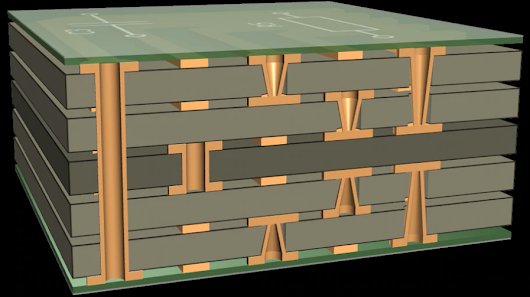
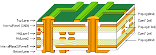
This posts delves into the specifics of PCB stack-up design with a focus on Design for Manufacturing (DFM) for 4, 6, and 8 layer PCBs. It explores how thoughtful design can significantly influence manufacturing efficiency, cost-effectiveness, and product reliability. By understanding the subtleties of stack-up design, electronics engineers and PCB designers can optimize their boards for both performance and manufacturing costs, navigating the complexities of PCB material choices, impedance control, and layer count implications with greater confidence.
Understanding The Multilayer PCB Stack-Up
What is PCB Stack-Up?
PCB stack-up refers to the arrangement of copper layers and insulating materials in a printed circuit board. This structure is crucial because it determines the electrical properties, thermal management, and mechanical stability of the PCB. A well-designed stack-up can enhance signal integrity, reduce electromagnetic interference (EMI), and manage power distribution more effectively.
Common Configurations
PCB stack-ups vary in complexity from simple single-layer boards to intricate multi-layer designs. The most common multi-layer configurations are:
- 4-Layer PCB Stackup: Typically consists of two signal layers and two planes (power and ground). This configuration is ideal for moderately complex circuits, offering a balance between cost and performance.
- 6-Layer PCB Stackup: Provides additional layers for improved shielding and routing space for complex circuits, usually involving four signal layers interspersed with power and ground planes.
- 8-Layer PCB Stackup: Ideal for advanced applications with high-density interconnects, providing ample layering for signal integrity and minimal cross-talk.
Each configuration has its specific uses, benefits, and design considerations, which will be explored in detail in the following sections.
DFM Design for PCB Stack-Up
Overview of DFM in PCB Manufacturing
Design for Manufacturing (DFM) is a critical practice in PCB design that ensures the manufacturability of the board while minimizing cost and maximizing efficiency. It involves designing PCBs in such a way that they are easy to manufacture without requiring excessive engineering changes during the production phase.
Designing a 4-Layer PCB Stack-Up
A 4-layer PCB is often the choice for designs that need more than a double-layer board but do not require the complexity of a 6 or 8-layer board. The typical stack-up configuration is:
This setup provides good EMC performance with minimal cost. By using only one core and two sheets of prepreg, a 4-layer board can be manufactured cost-effectively, balancing performance with production simplicity.
Designing a 6-Layer PCB Stack-Up
Moving to a 6-layer PCB allows for greater separation of power and ground planes from the signal layers, reducing EMI and improving signal integrity. The common stack-up might look like:
This configuration uses two cores and three sheets of prepreg, which increases the cost but provides better performance for more complex circuits.
Designing an 8-Layer PCB Stack-Up
An 8-layer PCB is used in high-density designs where additional layers are necessary for multiple power and ground layers or for intricate routing requirements. The typical configuration might include:
This arrangement, using three cores and four sheets of prepreg, significantly increases the material costs but is essential for achieving the desired electrical performance in advanced circuit electronic systems.
The next sections will build upon these configurations, discussing their impact on costs, the implications of design choices on PCB warpage, and more.
Cost Implications of Stack-Up Design
Cost Analysis of PCB Layers and Material Use
The cost of a PCB largely depends on the number of layers, the type and quantity of materials used (such as core and prepreg), and the complexity of the manufacturing processes involved. Here's how different stack-up designs impact the overall cost:
- 4-Layer PCB: Utilizing one core and two sheets of prepreg, a 4-layer PCB is generally the most cost-effective option for multi-layer boards. The use of a single core helps keep material costs down while providing sufficient functionality for many applications.
- 6-Layer PCB: This design typically uses two cores and three sheets of prepreg, increasing the material costs due to the additional core. The complexity of alignment during layering also adds to the manufacturing cost but offers better performance for complex circuits.
- 8-Layer PCB: With three cores and four sheets of prepreg, the 8-layer PCB is the most expensive among the three due to the high material usage and the intricate manufacturing process required to ensure layer alignment and reliability.
Practical Cost-Saving Strategies
To optimize the cost of manufacturing PCBs without compromising quality, designers can employ several strategies:
- Optimize layer count to match the complexity of the application.
- Choose materials judiciously based on performance requirements and cost.
- Design for manufacturability to reduce waste and streamline production processes.
- Adheres to the standard number of Core material (Typically a 4-layer stackup utilizes one core, a 6-layer stackup uses two cores, and an 8-layer stackup incorporates three cores. The use of more cores increases the cost of the PCB.)
Impact of Stack-Up Design on Warpage
Understanding PCB Warpage
How Stack-Up Design Influences Warpage
Tips for Reducing Warpage in PCB Design
- Maintain a balanced and symmetrical layer structure.
- Select materials with compatible thermal properties.
- Design with uniform copper density across all layers to prevent uneven heating and cooling.
Impedance Control in PCB Stack-Up
Significance of Impedance Control
How Impedance Requirements Affect PCB Stack-Up
Strategies for Achieving Desired Impedance
- Use consistent spacing between layers to maintain uniform impedance across the board.
- Select materials with stable dielectric constants under varying environmental conditions.
- Implement careful routing and placement of components to avoid impedance mismatches.
Material Selection for PCB Stack-Up
Types of Prepreg and Core Materials
Selection Criteria for Prepreg and Core Materials
- Consider thermal stability, dielectric constant, and mechanical strength.
- Balance performance requirements with cost constraints.
Deciding on Prepreg Adhesive Thickness
Role of Prepreg Adhesive Thickness in PCB Stack-Up
Guidelines for Selecting Adhesive Thickness
Conclusion: Optimizing PCB Design for Performance and Manufacturing
The intricate process of PCB stack-up design plays a fundamental role in determining the functionality, reliability, and manufacturability of electronic devices. As we have explored, each decision from the number of layers to the choice of materials impacts not just the electrical performance of the PCB but also its cost and susceptibility to issues like warpage.
For electronics engineers and PCB designers, achieving an optimal balance between complexity and cost efficiency requires a deep understanding of DFM principles and a strategic approach to material selection and layer configuration. By carefully designing a 4, 6, or 8 layer stack-up, designers can meet specific impedance requirements, minimize warpage, and ensure robust performance in the final product.
In conclusion, while the technical challenges of designing efficient PCB stack-ups are significant, the benefits of a well-considered design are profound. It not only enhances the product's performance but also streamlines the manufacturing process, reducing costs and improving yield rates. As technology advances, the principles of effective PCB design remain crucial in driving innovations and ensuring the success of electronic products in increasingly competitive markets.


