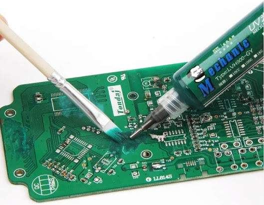
The solder mask serving as a thin protective layer that covers the majority of the circuit board's surface, the solder mask—also known as solder resist—plays a crucial role in ensuring both the functionality and longevity of the board. Its primary function is to prevent unintended solder bridges from forming between closely spaced solder pads, which can lead to short circuits and malfunctioning of the electronic components.
Beyond its protective attributes, the solder mask significantly influences the assembly process and the overall performance of the final product. Advances in this technology, including the development of inkjet and laser direct imaging techniques, have enhanced its precision and efficiency, aligning with the industry's move towards more compact and complex PCB designs. The ongoing evolution in solder mask technology not only supports higher density and higher frequency PCB applications but also drives the industry towards adopting more environmentally sustainable practices.
This post delves into the sophisticated world of solder masks, exploring their critical importance, technological advancements, and the standards governing their use. We will examine how these advancements contribute to enhanced PCB performance and reliability, particularly in high-density and high-frequency applications, and how the industry is shifting towards more sustainable practices.
Purpose and Importance of Solder Mask
Function of Solder Mask
The solder mask serves multiple critical functions in the lifecycle of a printed circuit board (PCB). Primarily, it acts as a protective barrier that guards the copper traces of the PCB from environmental factors such as dust, moisture, and oxidation, which can lead to corrosion over time. More importantly, the solder mask prevents the formation of solder bridges during the soldering process. Solder bridges occur when excess solder forms unintended connections between circuit elements, potentially causing short circuits and failures in electronic devices.
Moreover, the solder mask aids in the reduction of soldering errors by clearly defining where solder should be applied, improving manufacturing efficiency and reducing waste. It also provides a color contrast against the metal leads and pads, which is particularly useful during the inspection and testing phases of manufacturing, allowing for easy identification of flaws.
Testing Standards
Adherence to industry standards is paramount in PCB manufacturing, with specific requirements set forth for solder masks. The IPC SM 840 classifies solder masks based on their intended use and durability. This classification ensures that solder masks meet rigorous standards of thermal, chemical, and mechanical durability that align with the operational requirements of the final product.
For example, Class T solder masks are designed for general commercial use where the environment may not be harsh, whereas Class H is suitable for high-performance electronic products that are exposed to extreme environmental conditions. These standards are crucial for manufacturers to adhere to, ensuring reliability across various applications.
- Thermal Endurance: Solder masks must withstand high temperatures during both the soldering process and the operational phase of the PCB.
- Chemical Resistance: Effective resistance to the chemicals used in PCB manufacturing and operation, including cleaning agents and flux, is critical.
- Mechanical Durability: The solder mask must be robust enough to resist scratching and other physical damages during handling and use.
The implementation of these standards is crucial not only for the functionality and longevity of the PCBs but also for maintaining high yield rates in PCB manufacturing, ultimately affecting the cost-efficiency of production and the reliability of the final products.
Next, I will cover the industry standards for solder mask thickness, explaining the typical ranges and their applications across various types of PCBs. This will include details on how thickness standards are determined and why they are important for different manufacturing requirements.
Standard Industry Thickness and Spec
Thickness Guidelines
The thickness of a solder mask can vary significantly depending on the application requirements of the printed circuit board (PCB). Generally, the standard thickness of solder masks ranges from 20 to 40 microns. However, specific applications may require adjustments to this range to accommodate different design and performance criteria.- Insulation: Thicker solder masks provide better insulation, protecting against electrical shorts between closely spaced components.
- Surface Planarity: A uniform solder mask thickness helps maintain a level surface for the mounting of components, which is particularly important in high-density interconnect (HDI) boards.
- Durability: In environments where mechanical wear and abrasion are concerns, a thicker solder mask can offer enhanced protection, prolonging the life of the PCB.
Application-Specific Considerations
For standard applications, a thickness at the lower end of the range is often sufficient. However, for boards that are subject to harsher mechanical stresses or that require higher levels of insulation, the upper end of the thickness spectrum may be more appropriate.
- High-Density Applications: In HDI PCBs, where the spacing between components is minimal, maintaining a thinner solder mask can prevent issues related to bridging and short-circuiting.
- High-Frequency Applications: For high-frequency PCBs, the thickness of the solder mask must be carefully managed to avoid any adverse effects on the electrical properties of the board, such as impedance and capacitance.
Measurement and Compliance
The measurement of solder mask thickness is typically conducted using specialized equipment that can accurately gauge the coating on top of the copper traces and pads. It is essential for manufacturers to regularly verify this thickness to ensure compliance with both the design specifications and the relevant IPC standards.
Ensuring that the solder mask meets the specified thickness is vital not only for the functionality and reliability of the PCB but also for achieving optimal yield rates during manufacturing. By adhering to these standards, manufacturers can reduce the risk of defects, minimize rework, and maintain consistency across production batches.
Having detailed the industry standards for solder mask thickness and their importance in PCB manufacturing, I will next discuss how advancements in solder mask technology contribute to enhanced PCB performance and reliability, especially in high-density and high-frequency applications. This section will also explore the environmental impacts of different solder mask types and industry shifts towards more sustainable practices.
Technological Advancements in Solder Mask
Enhancements for High-Density Applications
- High-Frequency PCBs: For high-frequency applications, the properties of the solder mask, such as its dielectric constant and thickness, become even more critical. Advanced solder masks are designed to have minimal impact on signal integrity, reducing the risk of interference and signal loss which is paramount in high-frequency circuits.
Environmental and Sustainability Considerations
- UV Curable Solder Masks: These types of solder masks not only improve production efficiency by reducing curing times but also decrease energy consumption and environmental impact. UV curable masks require less energy and produce fewer emissions compared to traditional thermal curing processes.
Selecting Solder Mask Types
- High CTI Solder Mask: Materials with a high Comparative Tracking Index (CTI) are better suited for environments where high voltage and humidity can cause electrical tracking and failure.
- Halogen-Free Solder Masks: For applications requiring environmental and health safety, halogen-free solder masks are preferable as they do not release harmful halogens under high heat conditions.
- Flexibility and Durability: Different applications may require solder masks with specific mechanical properties, such as flexibility for flex circuits or extra durability for industrial applications.
Eco-Friendly Solder Mask Technologies
Definition and Benefits
- Reduced Environmental Toxins: By avoiding harmful chemicals like brominated flame retardants or PVC-based compounds, eco-friendly solder masks reduce the release of toxins into the environment during both the manufacturing and disposal phases of the PCB lifecycle.
- Lower Energy Consumption: Many eco-friendly solder masks are designed to cure at lower temperatures or through energy-efficient processes such as UV curing, which significantly reduces the energy consumption associated with their application and curing.
- Compliance with Environmental Regulations: Using eco-friendly solder masks helps manufacturers comply with increasingly stringent environmental regulations and meet the certification standards required in many markets, enhancing product marketability.
Growing Industry Adoption
- Innovative Materials: Recent innovations include the development of solder masks derived from bio-based resins or those that utilize water-based technologies, further reducing their environmental footprint.
- Market Differentiation: For PCB manufacturers, offering products made with eco-friendly solder masks can provide a competitive edge in markets where environmental sustainability is a significant concern among end-users.
Solder Mask Printing Processes
Overview of Methods
- Stencil Printing Method: This process involves applying the solder mask using a stencil made to match the PCB layout. The mask is spread over the stencil, and excess is removed, leaving the mask only in the desired areas. This method is particularly effective for large-scale productions where consistency and speed are critical.
- Spray Application Method: Spray methods utilize specialized equipment to spray the solder mask onto the PCB. This method provides a uniform and thin layer, which is ideal for high-density PCBs where precision is paramount. It is also adaptable to complex board shapes and sizes.
- Curtain Coating: Another method is curtain coating, where the solder mask is poured over the PCB as it passes under a curtain of the mask material. This technique is efficient for achieving a consistent thickness across the board.
- Dip Coating: In dip coating, the PCB is dipped into a tank containing the solder mask material, then withdrawn at a controlled rate to ensure a uniform coating. This method is suitable for boards requiring a thicker layer of solder mask.
- Screen Printing: This traditional method involves pressing ink through a fine mesh or screen that is patterned according to the PCB design. Screen printing is versatile and cost-effective but less precise than newer technologies, making it less ideal for very fine or complex patterns.
Innovations
- Laser Direct Imaging (LDI): LDI techniques allow for precise application of the solder mask without physical contact, using lasers to define the areas where the mask is needed. This method is excellent for complex, high-density PCBs where accuracy is critical.
- Inkjet Printing: Inkjet technology in solder mask application offers high precision and the ability to apply the mask selectively, reducing waste and processing time. This method is particularly useful for prototypes and small-batch productions where flexibility and customization are required.
Impact of Solder Mask Thickness on PCB Design
Impedance and Stack Up
- How Thickness Affects Impedance: The dielectric properties of the solder mask material and its thickness directly influence the impedance of the PCB. A thicker solder mask increases the distance between the signal layer and the reference plane, altering the impedance. This effect is particularly noticeable in controlled impedance applications, where maintaining consistent impedance values is crucial for the functionality of high-speed circuits.
- Stack-Up Considerations: In multi-layer PCBs, the overall stack-up — the arrangement and thickness of the various layers — must be carefully designed to achieve the desired electrical characteristics and mechanical stability. The solder mask is an integral part of this stack-up, and its thickness needs to be considered in the overall design to ensure that the board meets the required specifications.
Solutions and Adjustments
- Impedance Modeling and Simulation: Advanced modeling and simulation tools can predict how changes in solder mask thickness affect impedance. By simulating different scenarios, designers can optimize the solder mask application to meet specific impedance requirements before the manufacturing process begins.
- Material Selection: Choosing a solder mask material with appropriate dielectric properties is essential. Materials with lower dielectric constants may be preferable in designs where the solder mask thickness might impact impedance.
- Process Control: Maintaining strict control over the application process of the solder mask can help minimize variations in thickness. This includes choosing the right application method and regularly calibrating equipment to ensure consistent results.
- Design Adjustments: In some cases, adjustments to the PCB design may be necessary to compensate for the impedance effects of the solder mask. This could involve changing the layout of the signal paths or modifying the spacing between layers.


